semiconductor
0

0
Analog Layout Engineer Interview Questions | RC Matching & Routing CompensationIf you have four inverter standard cells (A, B, C, D) that are intended to ...
0

0
Analog Layout Mock Interview – 2+ Years Experience Introduction – “Tell me about yourself” https://youtu.be/aFMUU2zjGnQ Answer: “Hi, I have around 5 years of ...
0

0
What is Shielding? in Analog IC Layout design - VLSI semiconductor Sensitive nets such as clock nets, reset nets, analog signals, and high-speed data lines ...
0

0
How to Reduce Self-Heating Effect (SHE): 🧱 1. Use Better Thermal Conductive Materials Replace traditional SiO₂ or low-k dielectrics with materials that ...
0
0
Summary: Leakage Mechanisms in Half Dummy vs Full Dummy Analog Layout Designs Full Dummy Layout:Definition: Uses dummy (non-functional) devices on all sides ...
0
0
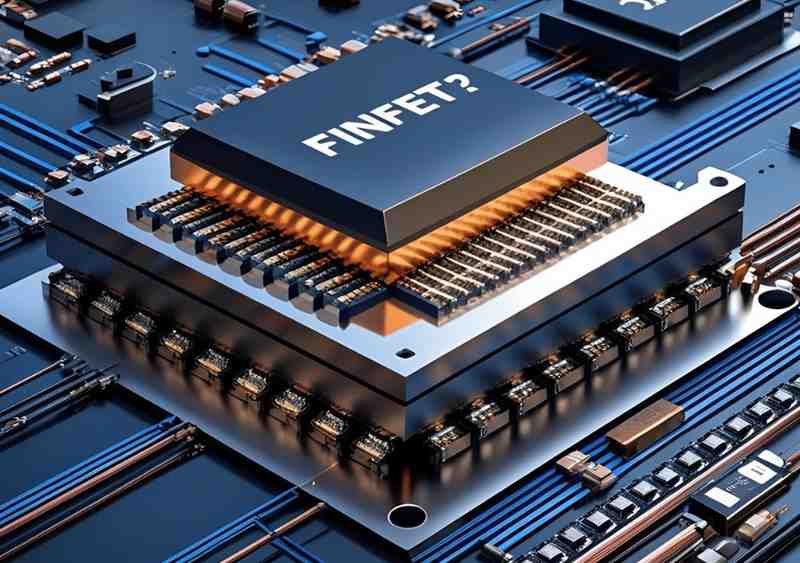
Why FinFET? Understanding the Shift from Planar to 3D Transistors As technology continues to scale below 22nm, traditional planar transistors are starting to ...
0

0
What is AI? Understanding the Basics and Exploring Its TypesArtificial Intelligence, or AI, is one of those buzzwords that seems to be everywhere these days. ...
0
0
How AI is Revolutionizing Analog IC Layout Design: Tools, Techniques, and BenefitsAI can significantly enhance analog IC (integrated circuit) layout design ...
0

0
How can I minimize inductive parasitics?Minimizing inductive parasitics in analog layout design is crucial for avoiding unwanted effects such as ...
0
0
Can you explain more about resistive parasitics?Certainly! Resistive parasitics in analog layout refer to the unwanted resistances that exist in the ...